株式会社オプトサイエンス野田工場
〒278-0015 千葉県野田市西三ヶ尾市橋90
TEL:04-7125-2508 FAX:04-7124-1186
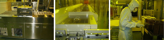
>> 高品質と超高精細加工技術で、パターニング致します。
>> Patterning with high quality and ultra-high precision
processing technology
STN液晶向け高精細パターン加工
パッシブOLED向けパターン加工
FFS用パターン加工
IPS用パターン加工
静電容量タッチパネル向けパターン加工
OLED照明向けパターン加工
航空機用(AVIONICS)ヒーターガラス、カバーガラスの印刷、アッセンブリ
IHスポットリフロー加工
High precision patterning proccessing for STN(Super Twisted Nematic) LCD
Patterning proccessing for Passive OLED Device
Patterning proccessing for FFS(Fringe Field Switching) Device
Patterning proccessing for IPS(In Plane Switching) Device
Patterning proccessing for Capacitive touch panel
Patterning proccessing for OLED lighting
Heater glass,Cover glass,printing,assembly for Airplane(AVIONICS)
IH Spot Reflow
最小線間:ミクロンサイズから対応します
Min. 8μmから/8インチウェハーに限って3μm以上可能
対応膜:ITO膜,各種補助金属膜
ガラスサイズ:300x300〜420mm
別途サイズによってはご相談させて頂きます
板厚:0.3t〜1.1tまで
1.1t以上の場合、別途ご相談
又、0.3t以下についても別途ご相談
Pattern's Line and Space(L/S)
Min. 8μm/8μm,3/3 for only 8inch Wefer
Etchable thin film:ITO,MAM(MoNb/AlNd/MoNb),APC,Cr and more Metal films
Etchable size:300x300〜420mm Other size Please contact us
Etchable Sheet thickness:0.3t〜1.1t
Under 0.3t or over 1.1t Please contact us